Proton Calorimetry/Experimental Runs/2022/MayLED: Difference between revisions
SaadShaikh (talk | contribs) No edit summary |
SaadShaikh (talk | contribs) No edit summary |
||
| Line 4: | Line 4: | ||
'''Notes''' | '''Notes''' | ||
* | *DDC232 settings: 170us integration time and measured 10000 samples per run. | ||
*Signal Generator settings: 0 ps delay, 500 kHz, 300 ns width, 5 ns leading edge and trailing edge, 6V high, 0V low. | |||
*Fibres used: 25 and 29 (25 used for single injection tests). | |||
*Sheets used: 84, 82, 81, 80, 79, 78, 77, 76, 75 | |||
*Materials tested: none, white paper (0.01 mm thick), black card (0.02 mm thick), mylar foil (0.0012 mm thick). Materials cut into 10 cm x 10 cm layers and placed in-between sheets. | |||
{|class="wikitable" | {|class="wikitable" | ||
| Line 11: | Line 15: | ||
!Graph | !Graph | ||
|- | |- | ||
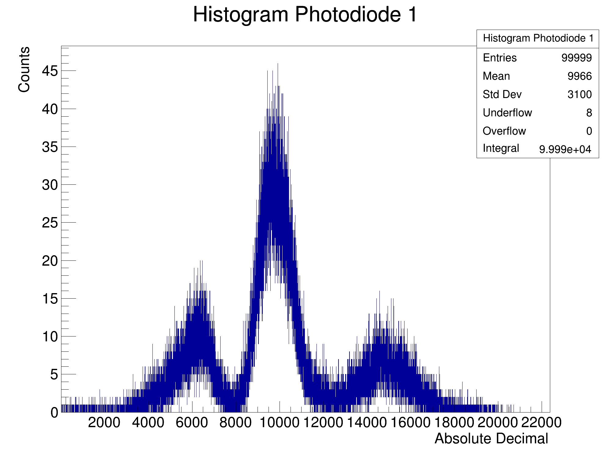
|1 || | |1 || No material dark noise test|| | ||
<div class="image150px" style="text-align: center;"> | <div class="image150px" style="text-align: center;"> | ||
[http://www.hep.ucl.ac.uk/pbt/wikiData/movies/DDC232/210422/Histograms/Run001.png http://www.hep.ucl.ac.uk/pbt/wikiData/movies/DDC232/210422/Histograms/Run001.png] | [http://www.hep.ucl.ac.uk/pbt/wikiData/movies/DDC232/210422/Histograms/Run001.png http://www.hep.ucl.ac.uk/pbt/wikiData/movies/DDC232/210422/Histograms/Run001.png] | ||
Revision as of 09:31, 16 May 2022
Optical isolation tests using LED fibre in D27.
Aim: Investigate optimal material to use to optically isolate unpainted sheets and whether single layers of material provide sufficient isolation.
Notes
- DDC232 settings: 170us integration time and measured 10000 samples per run.
- Signal Generator settings: 0 ps delay, 500 kHz, 300 ns width, 5 ns leading edge and trailing edge, 6V high, 0V low.
- Fibres used: 25 and 29 (25 used for single injection tests).
- Sheets used: 84, 82, 81, 80, 79, 78, 77, 76, 75
- Materials tested: none, white paper (0.01 mm thick), black card (0.02 mm thick), mylar foil (0.0012 mm thick). Materials cut into 10 cm x 10 cm layers and placed in-between sheets.
| Run | Description | Graph |
|---|---|---|
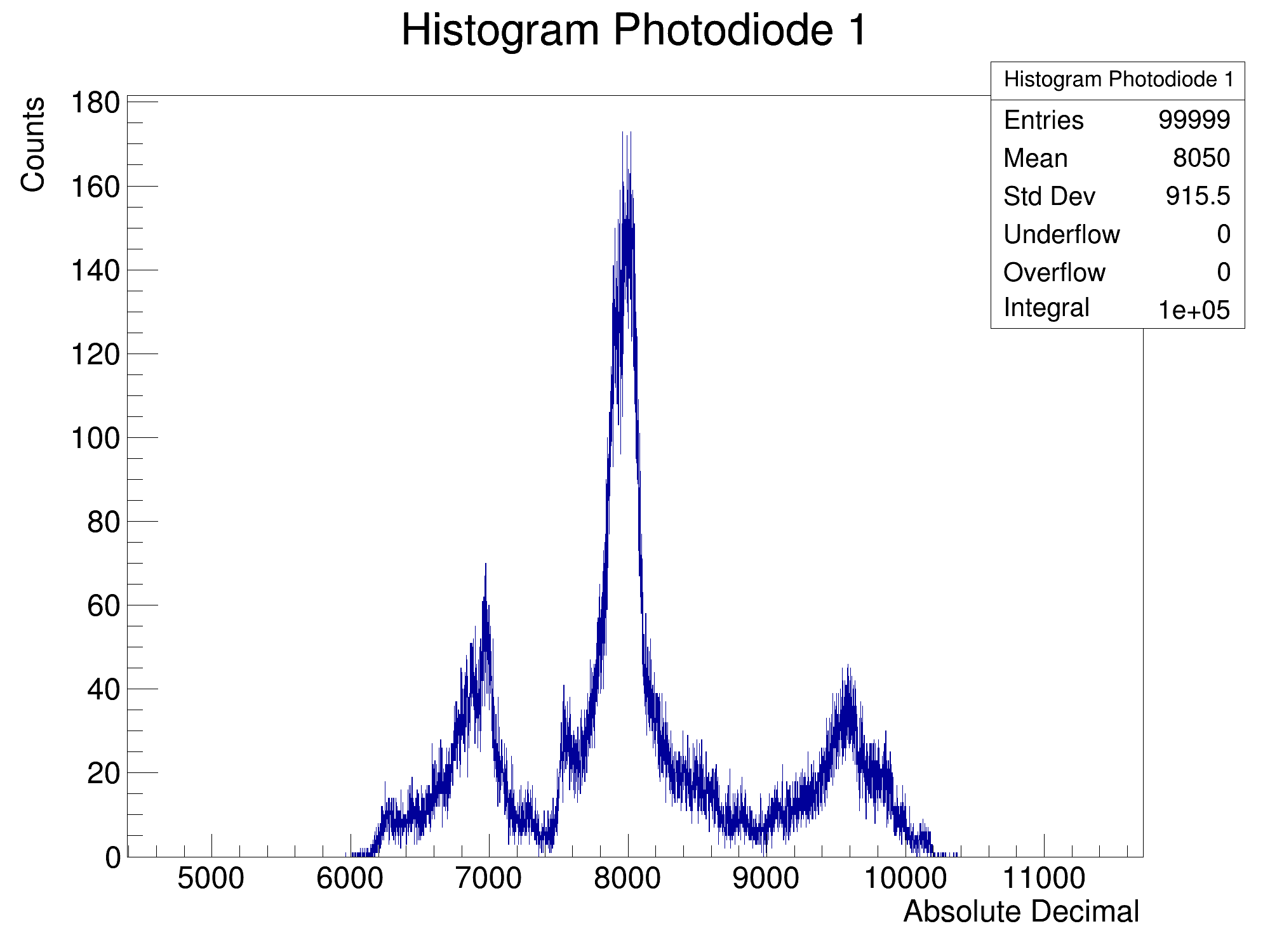
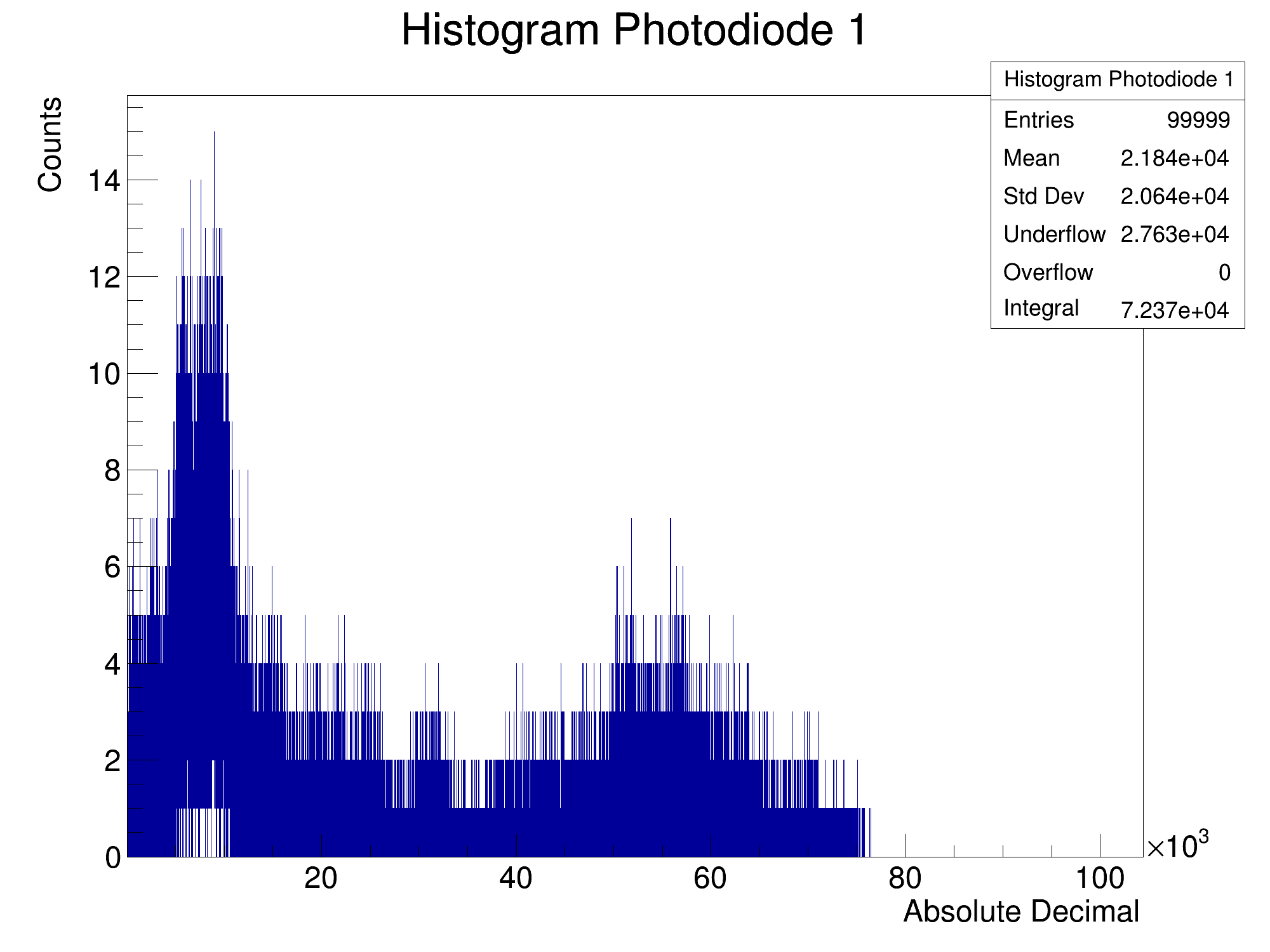
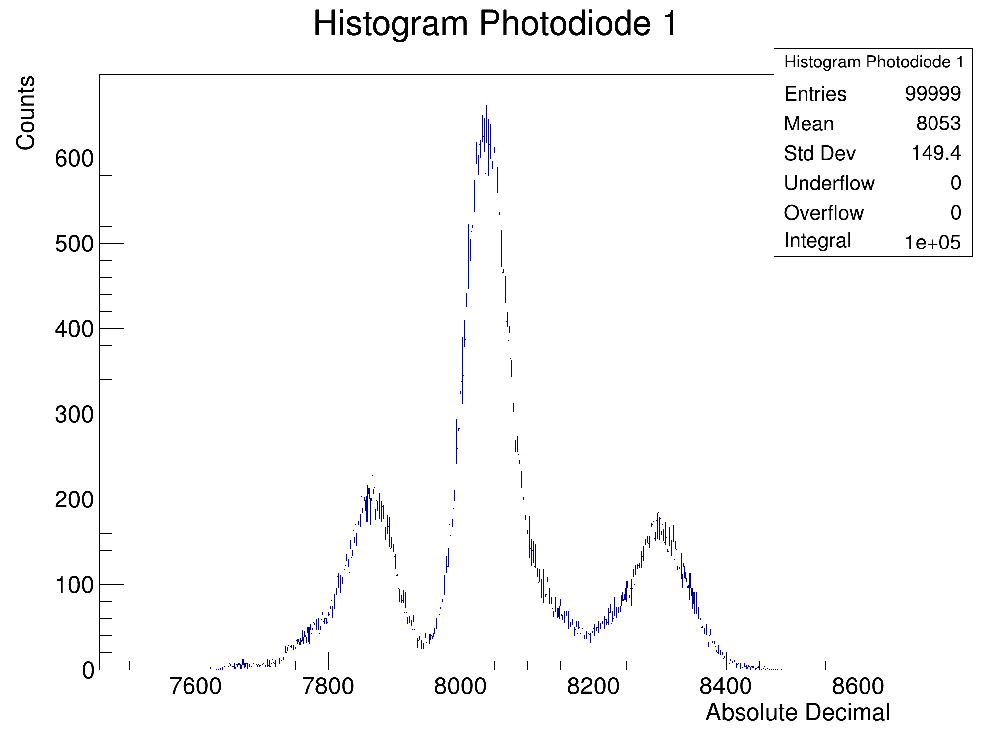
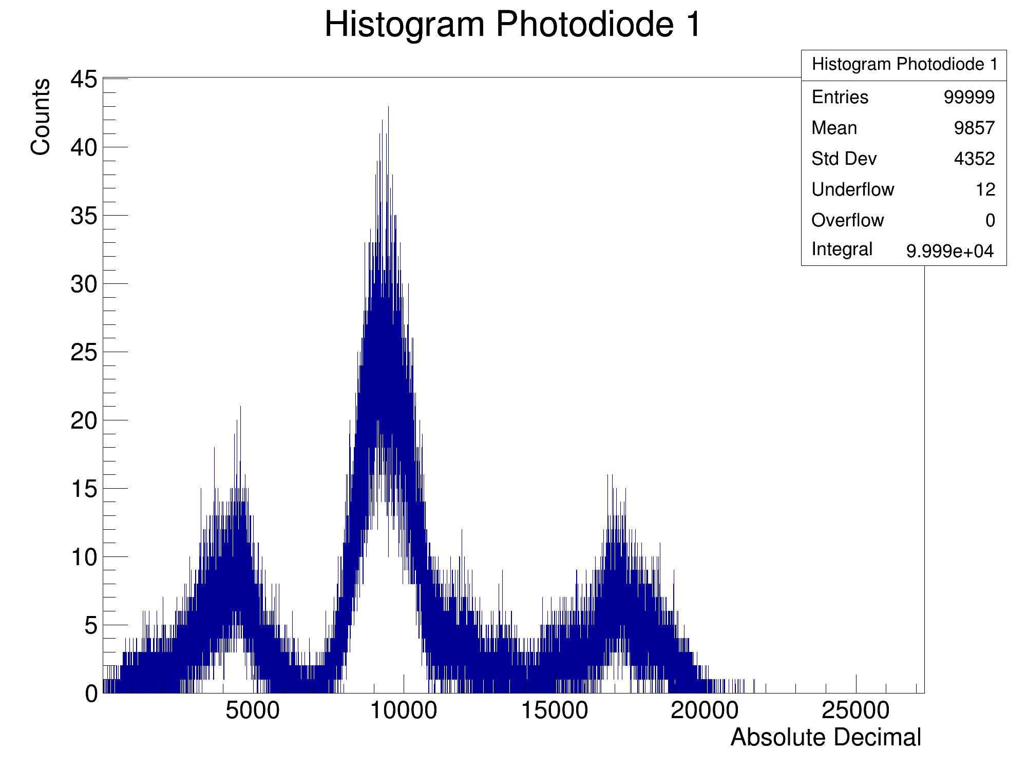
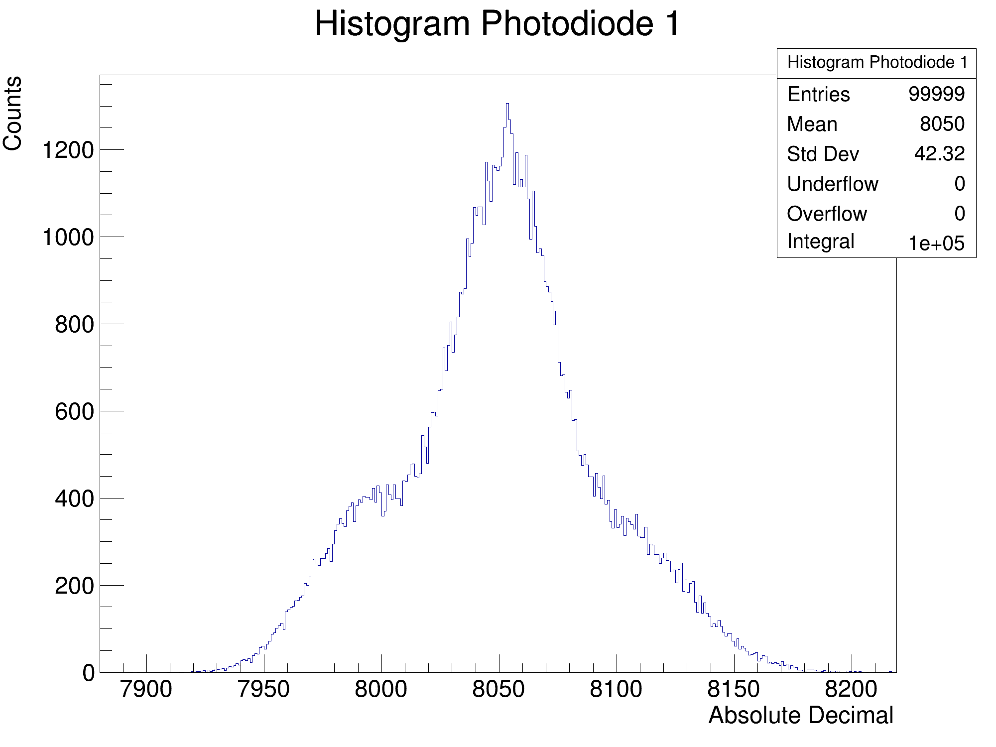
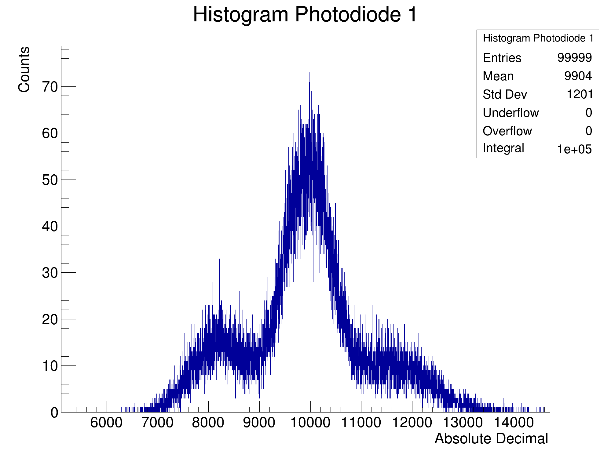
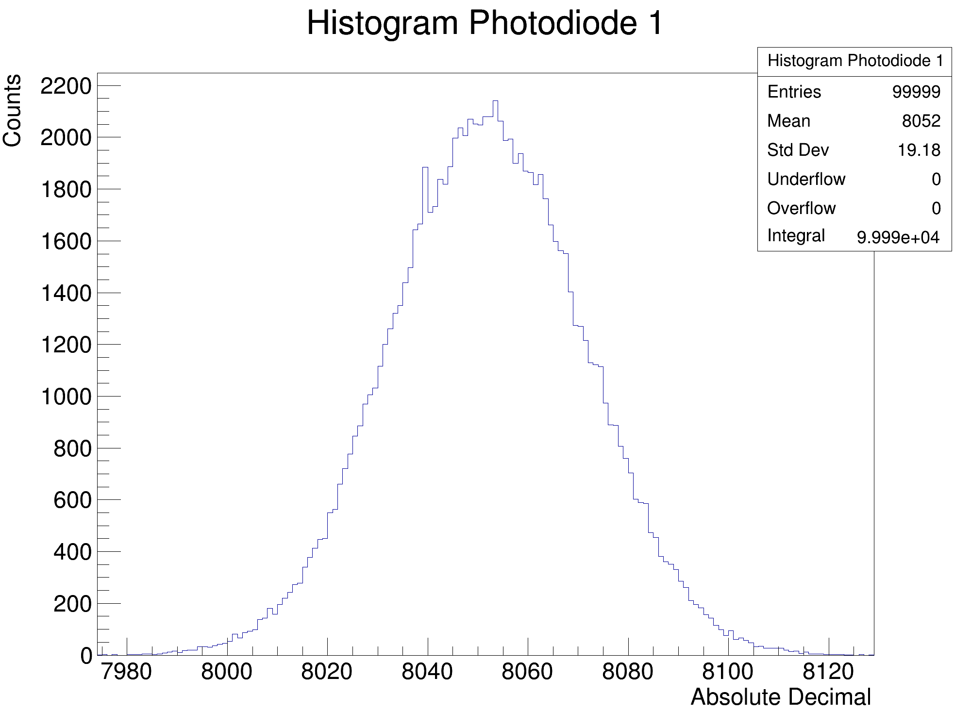
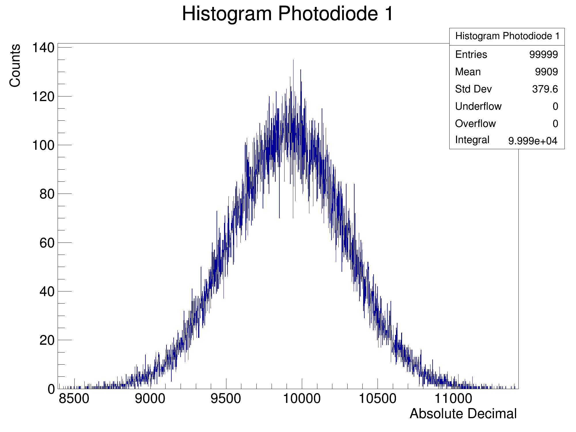
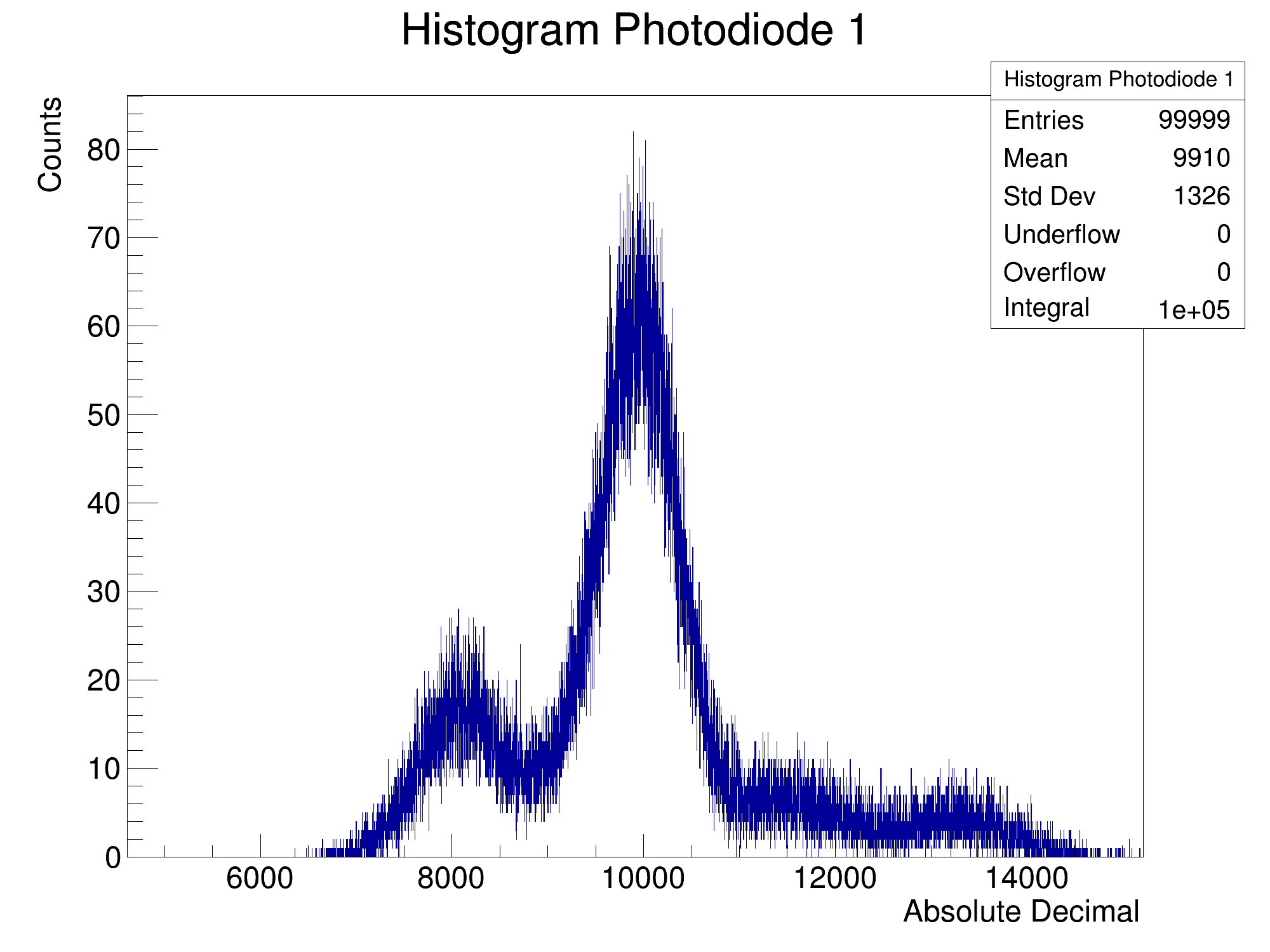
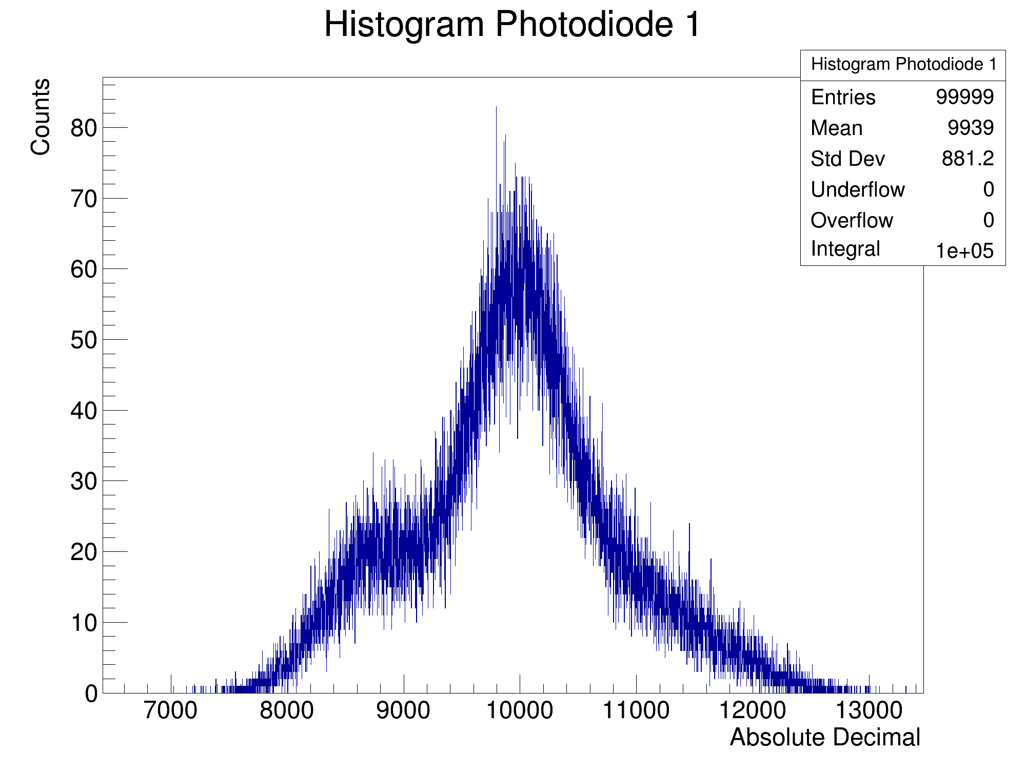
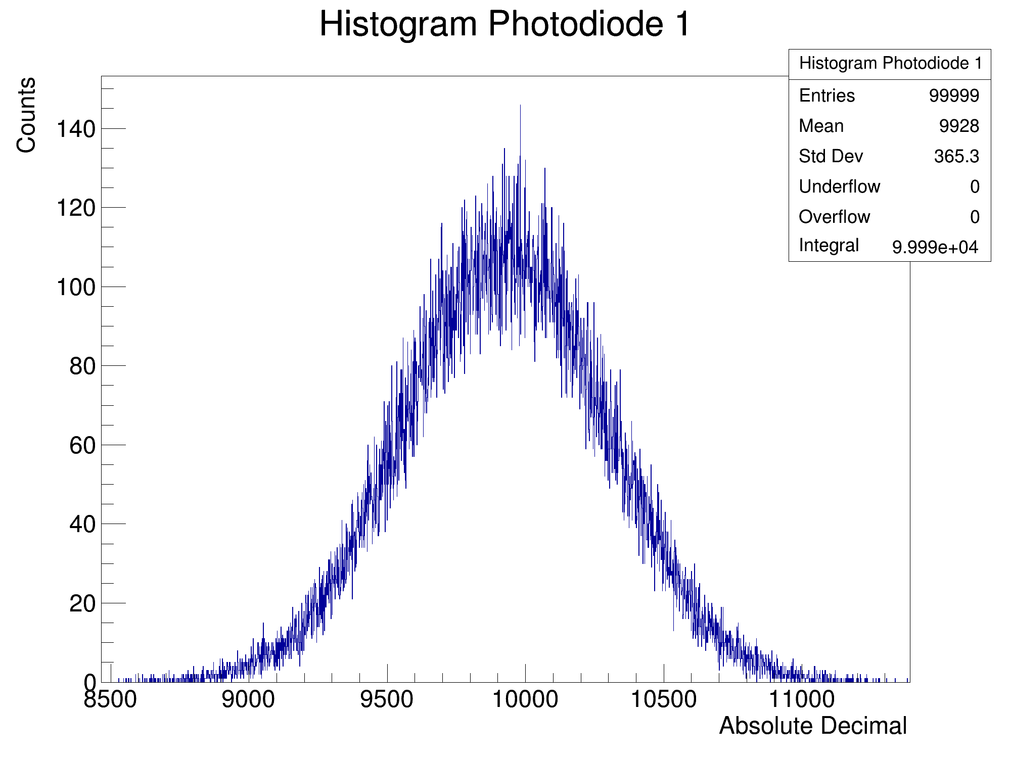
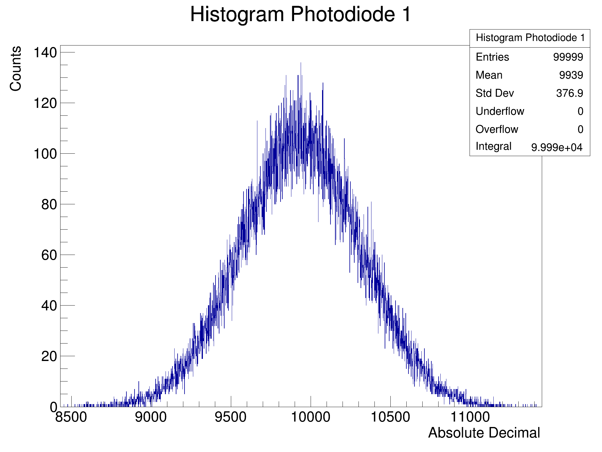
| 1 | No material dark noise test | |
| 2 | D27, CMOS on, 12.5pC | |
| 3 | D27, CMOS off, 350pC | |
| 4 | D27, CMOS off, 12.5pC | |
| 5 | D109, CMOS on, 350pC | |
| 6 | D109, CMOS on, 12.5pC | |
| 7 | D109, CMOS off, 350pC | |
| 8 | D109, CMOS off, 12.5pC | |
| 9 | D109, CMOS on, 12.5pC. Detector housing grounded using ground pin of FPGA. Grounded using optical breadboard inside detector. | |
| 10 | D109, CMOS on, 12.5pC. Previous grounding seemed ineffective. Now grounded by attaching clip to metal on outside face of detector enclosure. | |
| 11 | D109, CMOS off, 12.5pC, grounded. | |
| 12 | D27, CMOS off, 12.5pC, grounded. | |
| 13 | D27, CMOS off, 12.5pC | |
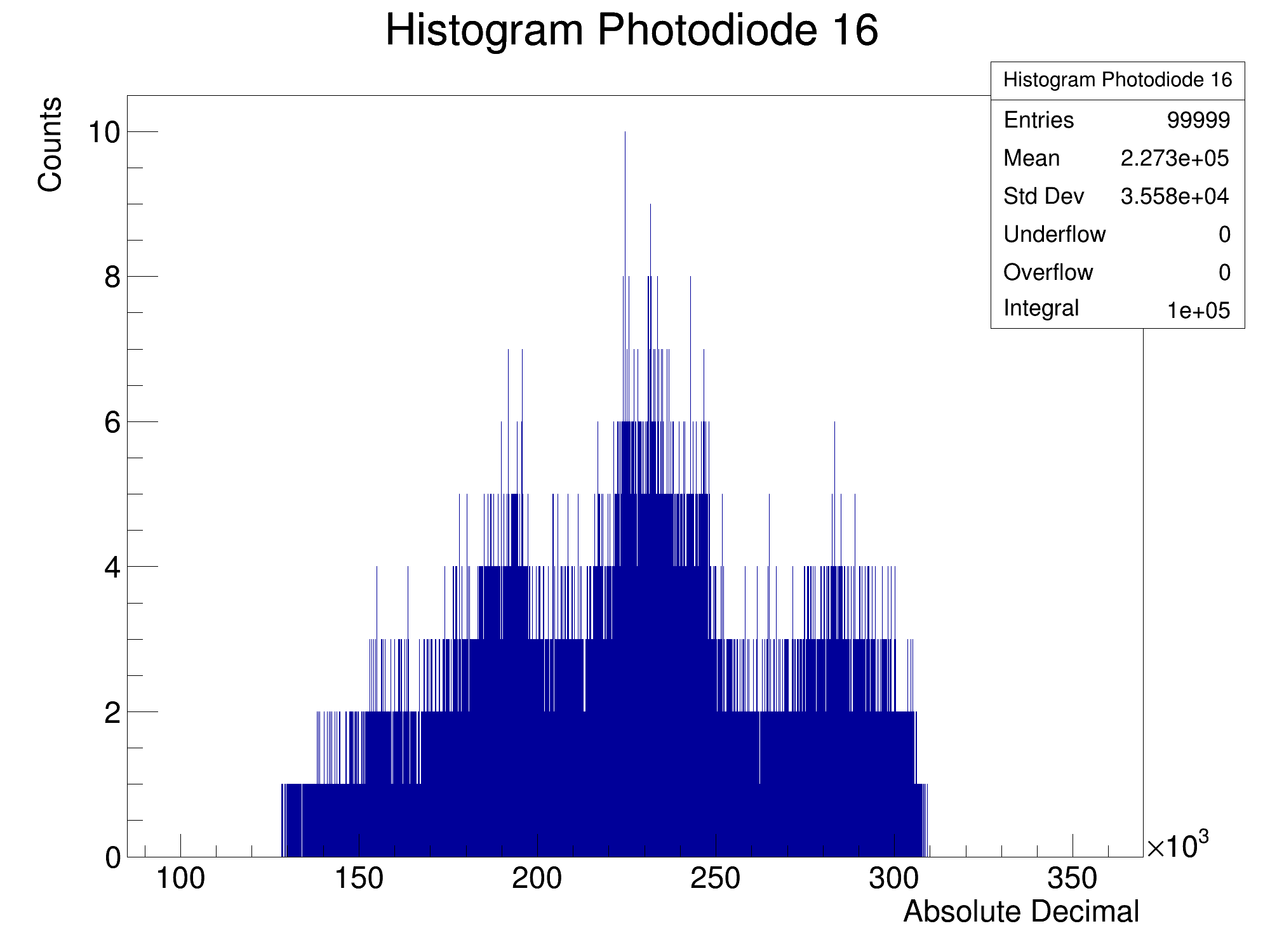
| 14 | D27, CMOS off, 12.5pC, grounded, LED. LED pulse of 1MHz, 6V height and 500ns width. Injected into single scintillator sheet coupled to photodiode 16. |
