Proton Calorimetry/Experimental Runs/2021/Apr1: Difference between revisions
SaadShaikh (talk | contribs) No edit summary |
SaadShaikh (talk | contribs) No edit summary |
||
| Line 30: | Line 30: | ||
[http://www.hep.ucl.ac.uk/pbt/wikiData/images/DDC232/20210401/IMG_3553.JPG http://www.hep.ucl.ac.uk/pbt/wikiData/images/DDC232/20210401/IMG_3553.JPG]</div> | [http://www.hep.ucl.ac.uk/pbt/wikiData/images/DDC232/20210401/IMG_3553.JPG http://www.hep.ucl.ac.uk/pbt/wikiData/images/DDC232/20210401/IMG_3553.JPG]</div> | ||
|- | |- | ||
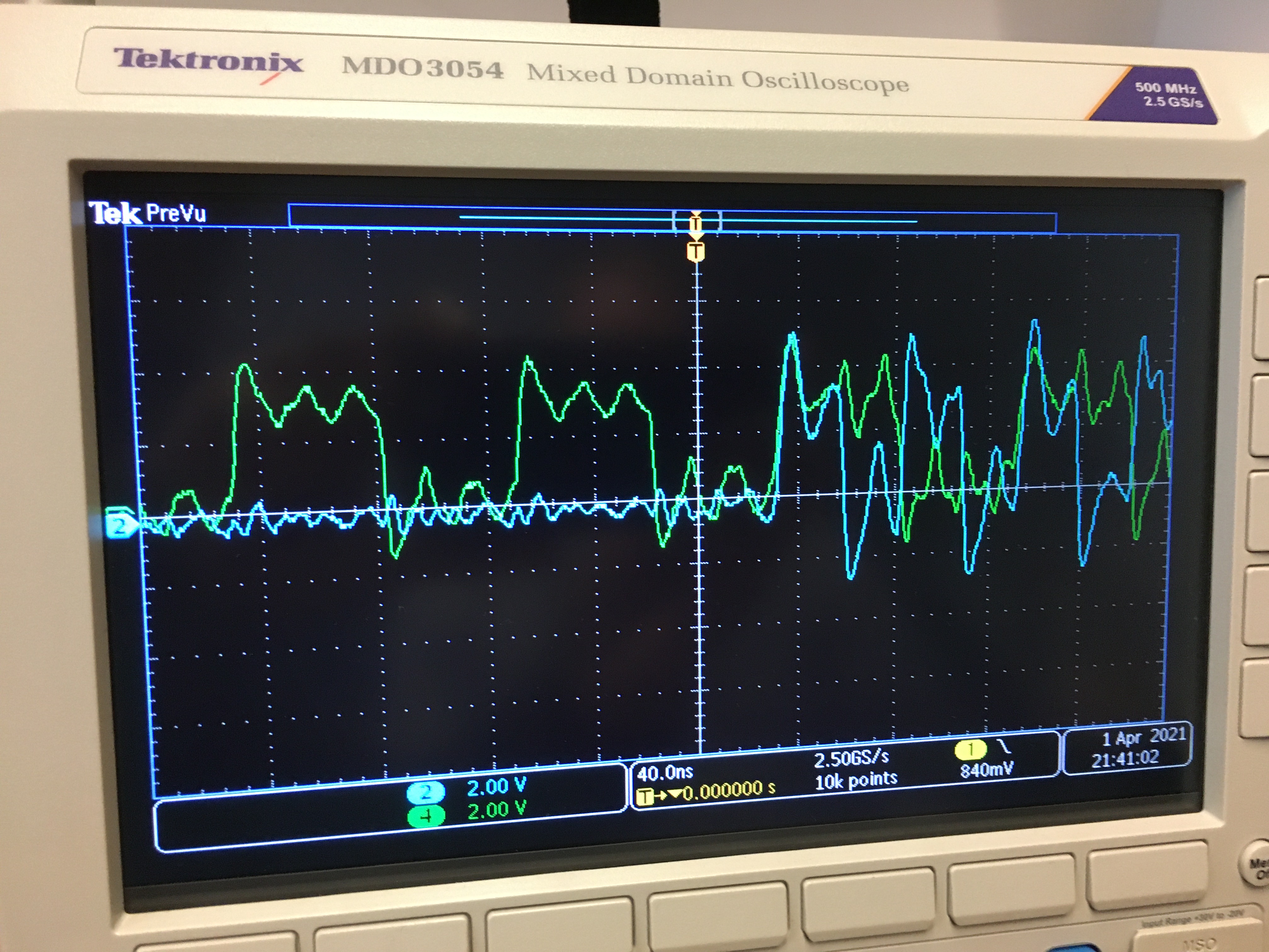
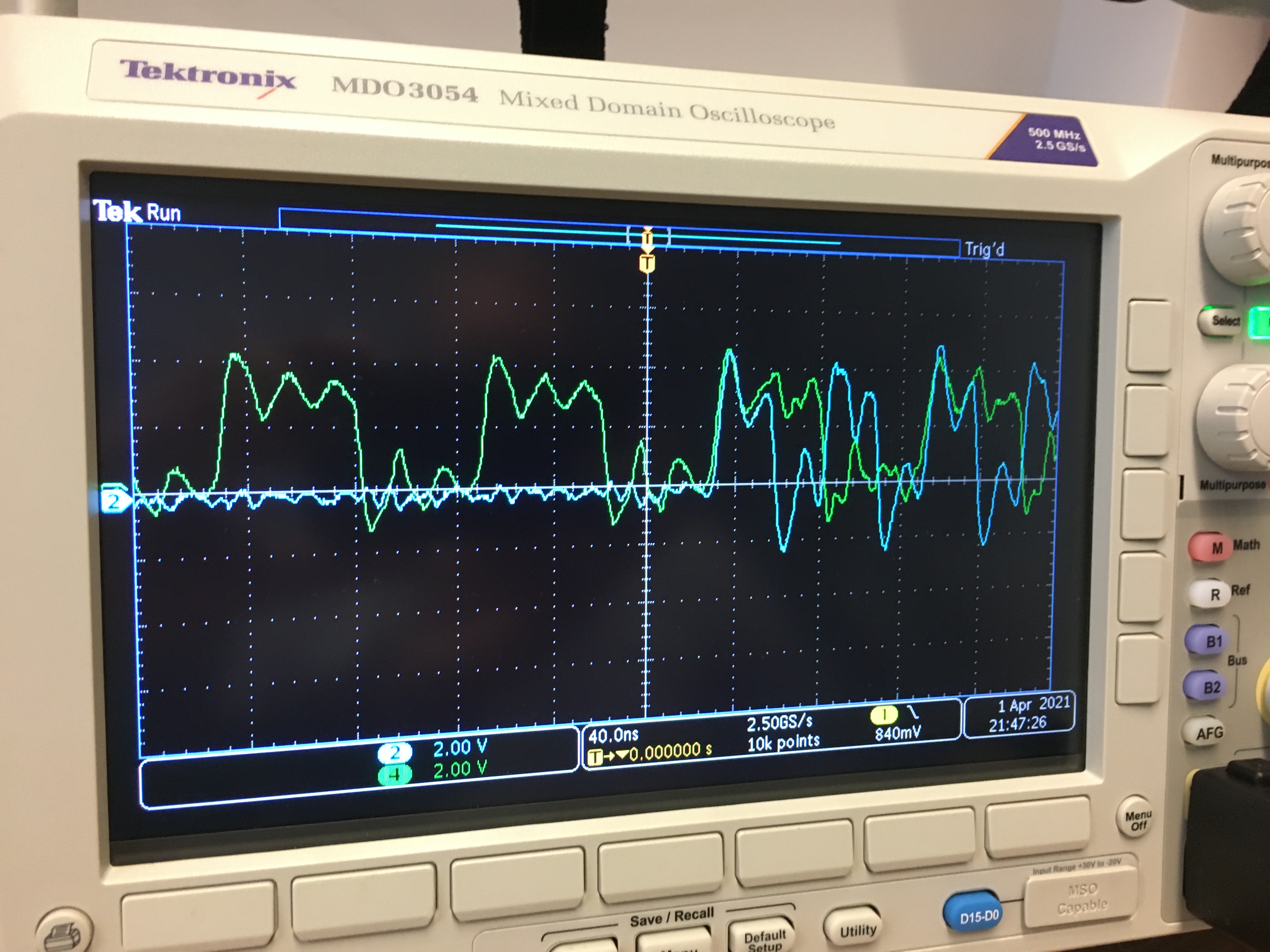
|4 || | |4 || P || Green trace shows CLK at J2 of DDC232 board, blue trace shows DCLK at J2 of DDC232 board. || <div class="image150px" style="text-align: center;"> | ||
[http://www.hep.ucl.ac.uk/pbt/wikiData/ | [http://www.hep.ucl.ac.uk/pbt/wikiData/images/DDC232/20210401/IMG_3554.JPG http://www.hep.ucl.ac.uk/pbt/wikiData/images/DDC232/20210401/IMG_3554.JPG]</div> | ||
|- | |- | ||
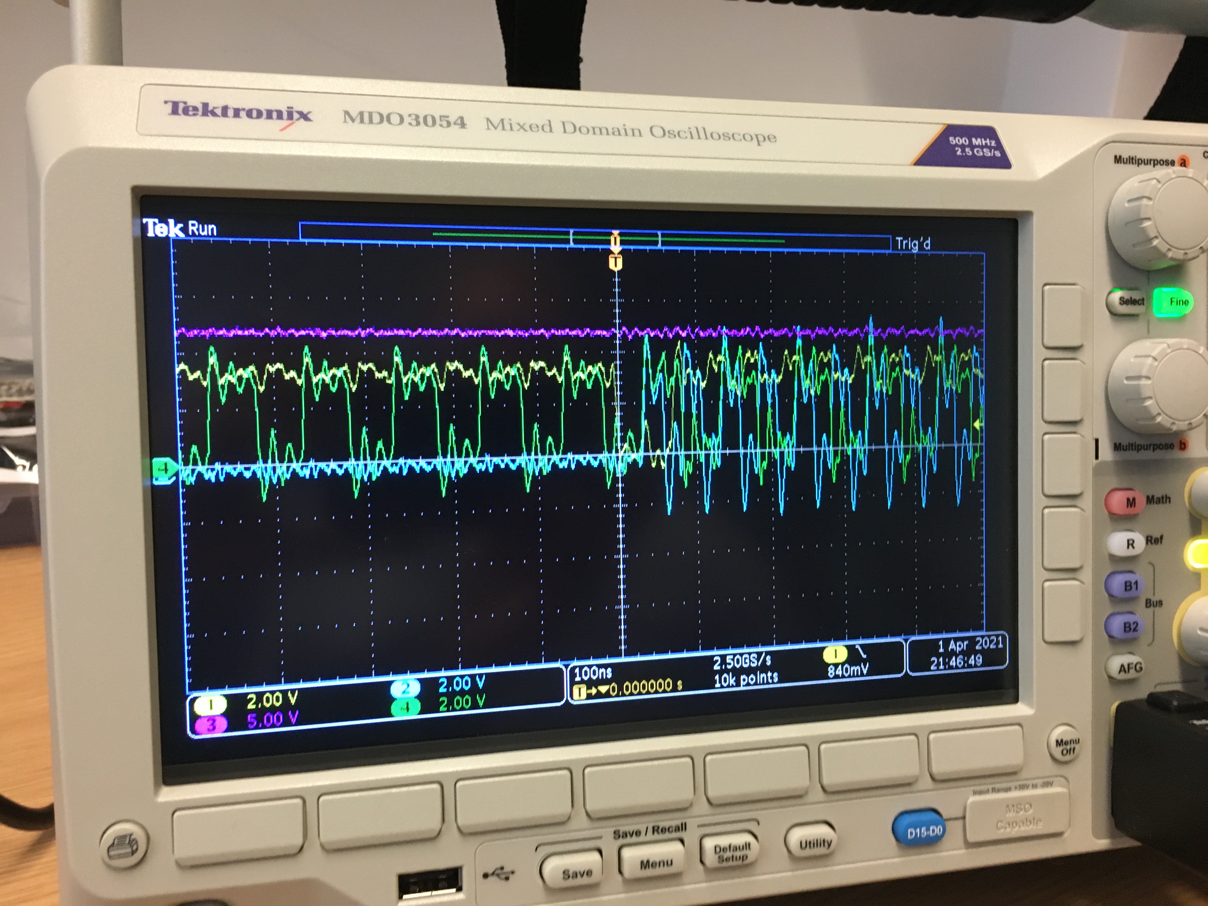
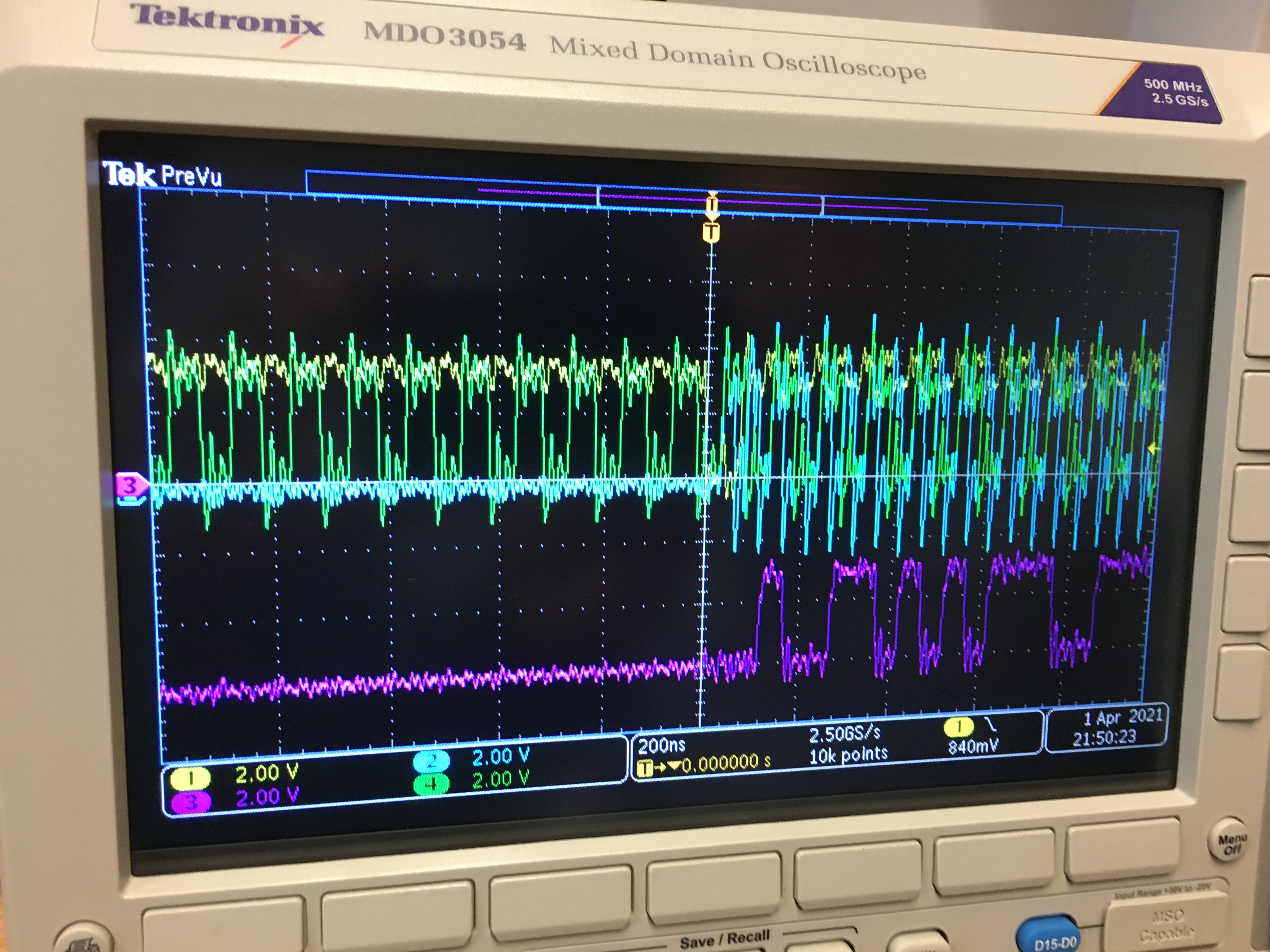
|5 || | |5 || P, P || Yellow trace shows DVALID at FPGA, green shows CLK of 1st board at J2, blue shows DCLK of 1st board at J2, purple shows 12V of 1st board at J2. || <div class="image150px" style="text-align: center;"> | ||
[http://www.hep.ucl.ac.uk/pbt/wikiData/ | [http://www.hep.ucl.ac.uk/pbt/wikiData/images/DDC232/20210401/IMG_3555.JPG http://www.hep.ucl.ac.uk/pbt/wikiData/images/DDC232/20210401/IMG_3555.JPG]</div> <div class="image150px" style="text-align: center;"> | ||
[http://www.hep.ucl.ac.uk/pbt/wikiData/images/DDC232/20210401/IMG_3556.JPG http://www.hep.ucl.ac.uk/pbt/wikiData/images/DDC232/20210401/IMG_3556.JPG]</div> | |||
|- | |- | ||
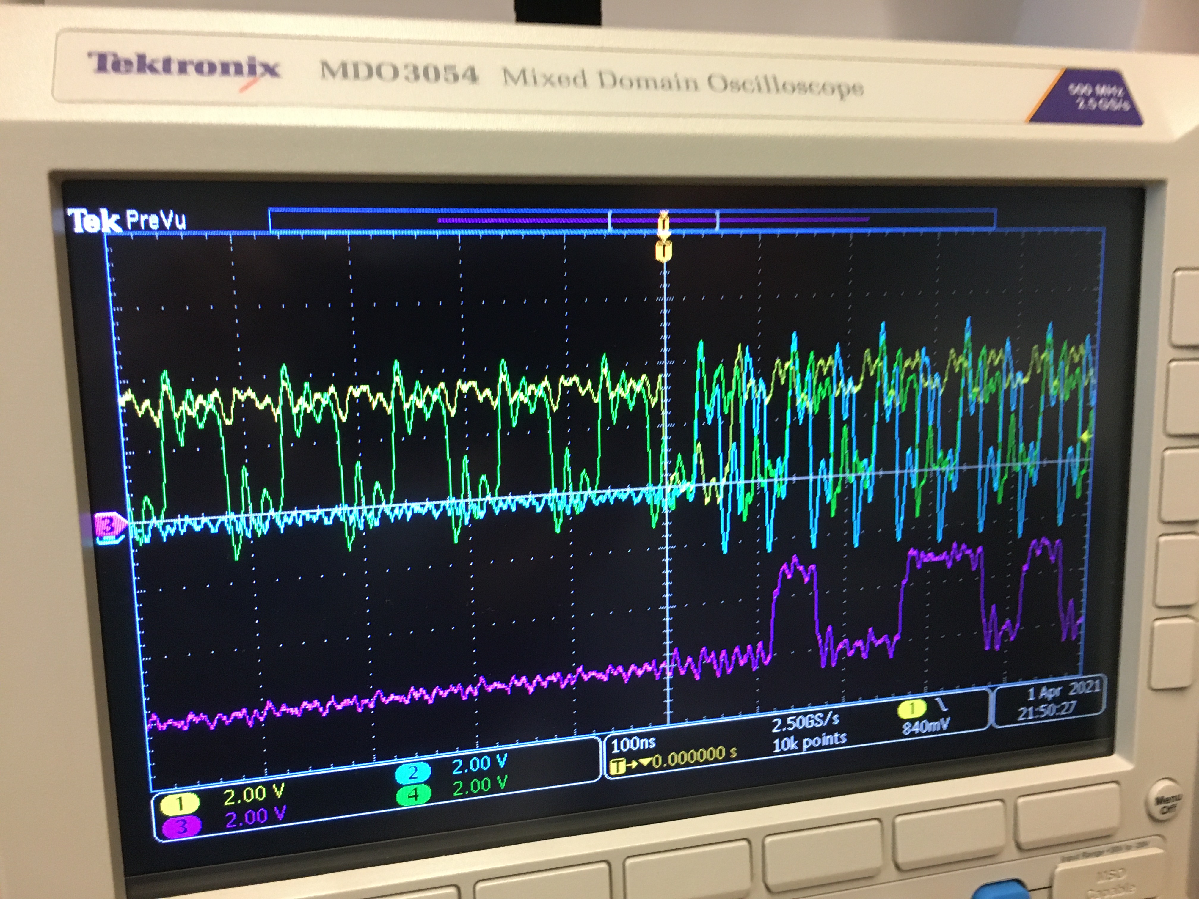
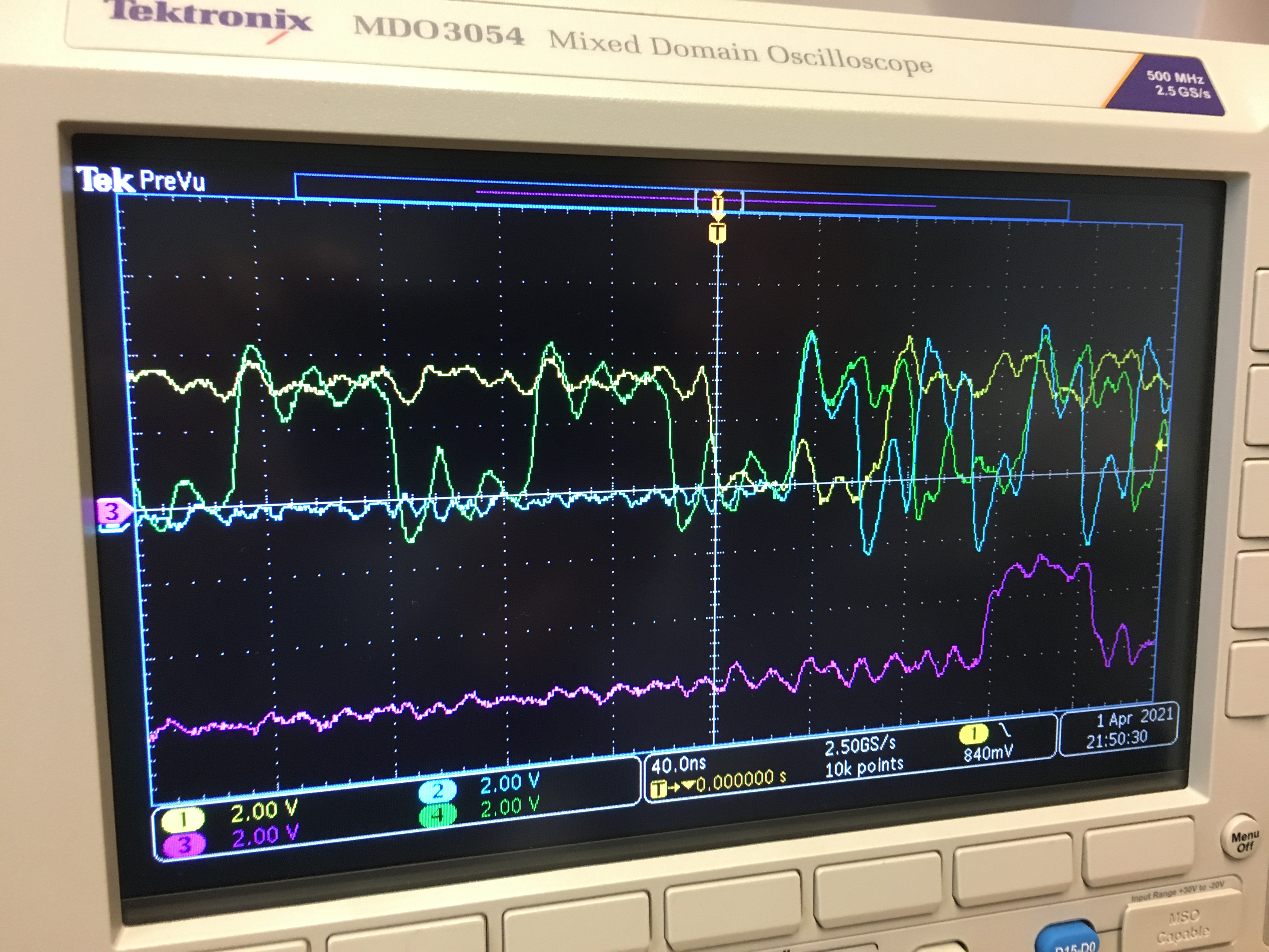
|6 || | |6 || P, P || Yellow trace shows DVALID at FPGA, green shows CLK of 1st board at J2, blue shows DCLK of 1st board at J2, purple shows DOUT of 1st board at J2. || <div class="image150px" style="text-align: center;"> | ||
[http://www.hep.ucl.ac.uk/pbt/wikiData/ | [http://www.hep.ucl.ac.uk/pbt/wikiData/images/DDC232/20210401/IMG_3557.JPG http://www.hep.ucl.ac.uk/pbt/wikiData/images/DDC232/20210401/IMG_3557.JPG]</div> <div class="image150px" style="text-align: center;"> | ||
[http://www.hep.ucl.ac.uk/pbt/wikiData/images/DDC232/20210401/IMG_3558.JPG http://www.hep.ucl.ac.uk/pbt/wikiData/images/DDC232/20210401/IMG_3558.JPG]</div> <div class="image150px" style="text-align: center;"> | |||
[http://www.hep.ucl.ac.uk/pbt/wikiData/images/DDC232/20210401/IMG_3559.JPG http://www.hep.ucl.ac.uk/pbt/wikiData/images/DDC232/20210401/IMG_3559.JPG]</div> <div class="image150px" style="text-align: center;"> | |||
[http://www.hep.ucl.ac.uk/pbt/wikiData/images/DDC232/20210401/IMG_3560.JPG http://www.hep.ucl.ac.uk/pbt/wikiData/images/DDC232/20210401/IMG_3560.JPG]</div> | |||
|- | |- | ||
|7 || 3, 4, 1 || Swept uncovering of each photodiode in turn - in opposite direction to run 6 - followed by board rotation and swept covering with finger. Note that board 4 shows zero output during uncovering due to signal dropouts associated with rotation. Low signals around 1m25s mark are a results of covering photodiodes partially with a finger. || <div class="image150px" style="text-align: center;"> | |7 || 3, 4, 1 || Swept uncovering of each photodiode in turn - in opposite direction to run 6 - followed by board rotation and swept covering with finger. Note that board 4 shows zero output during uncovering due to signal dropouts associated with rotation. Low signals around 1m25s mark are a results of covering photodiodes partially with a finger. || <div class="image150px" style="text-align: center;"> | ||
[http://www.hep.ucl.ac.uk/pbt/wikiData/ | [http://www.hep.ucl.ac.uk/pbt/wikiData/images/DDC232/20210401/IMG_3554.JPG http://www.hep.ucl.ac.uk/pbt/wikiData/images/DDC232/20210401/IMG_3554.JPG]</div> | ||
|- | |- | ||
|8 || 4, 3, 1 || Swept uncovering of each photodiode in turn followed by board rotation and swept covering with finger. Repeat of run 7 above but with board reordering. Note that board 4 <b>no longer shows noise when rotated</b> now that its the last board in the chain. || <div class="image150px" style="text-align: center;"> | |8 || 4, 3, 1 || Swept uncovering of each photodiode in turn followed by board rotation and swept covering with finger. Repeat of run 7 above but with board reordering. Note that board 4 <b>no longer shows noise when rotated</b> now that its the last board in the chain. || <div class="image150px" style="text-align: center;"> | ||
[http://www.hep.ucl.ac.uk/pbt/wikiData/ | [http://www.hep.ucl.ac.uk/pbt/wikiData/images/DDC232/20210401/IMG_3554.JPG http://www.hep.ucl.ac.uk/pbt/wikiData/images/DDC232/20210401/IMG_3554.JPG]</div> | ||
|- | |- | ||
|9 || 3, 4, 2 || Rotation of boards followed by swept covering of a few photodiodes in turn with black cloth. Now includes board 2 with resistor-shorted photodiode connections. Note that neither boards 4 or 2 show any output, corroborating that low values are mirrored despite board 4 being exposed to light. || <div class="image150px" style="text-align: center;"> | |9 || 3, 4, 2 || Rotation of boards followed by swept covering of a few photodiodes in turn with black cloth. Now includes board 2 with resistor-shorted photodiode connections. Note that neither boards 4 or 2 show any output, corroborating that low values are mirrored despite board 4 being exposed to light. || <div class="image150px" style="text-align: center;"> | ||
Revision as of 11:28, 7 April 2021
Daisy chain tests of second DDC232 prototype in D109
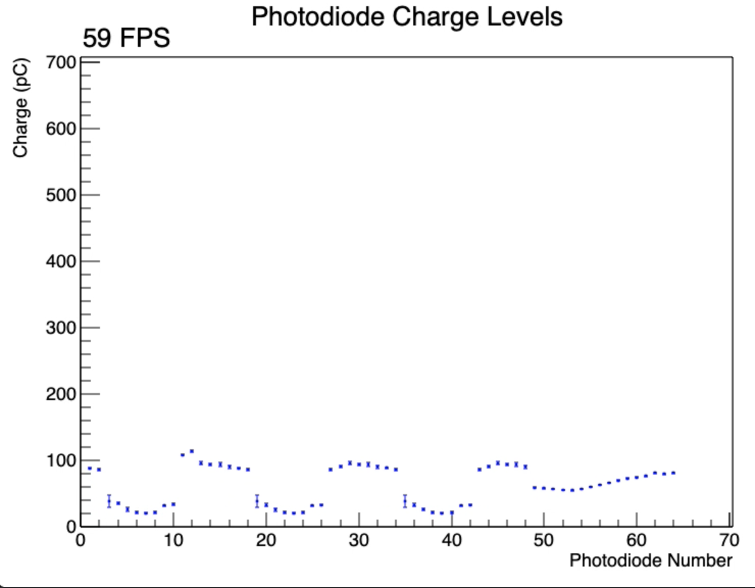
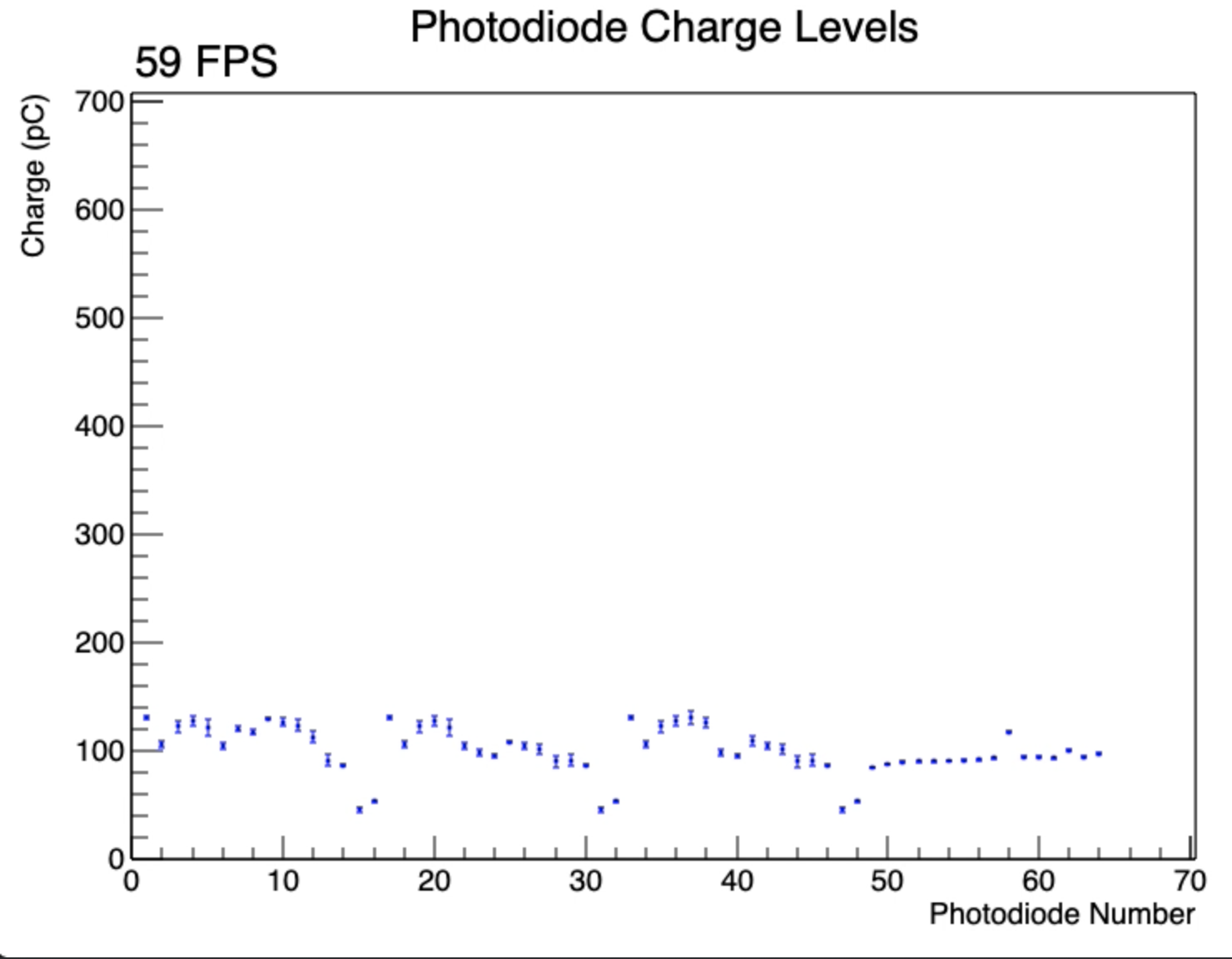
Aim: Debug "mirroring" issues when daisy-chaining more than 2 DDC232s boards. Test signal quality across boards using 500MHz oscilloscope.
Notes
- 3 DDC232 boards have S12915-16R photodiodes.
- 4th DDC232 board has 1k ohm resistors.
- In the runs below, boards are enumerated right to left, with the right-most board (1st board) connected to the FPGA.
- In the configuration column, P = board with photodiodes and R = board with resistors. The first board listed in this column is connected to the FPGA.
- In all runs, an integration time of 170us and full-scale range of 350pC is used.
Traces saved in /unix/www/html/pbt/wikiData/images/DDC232/20210401
| Run | Board Configuration | Scope Trace Description | Oscilloscope Trace |
|---|---|---|---|
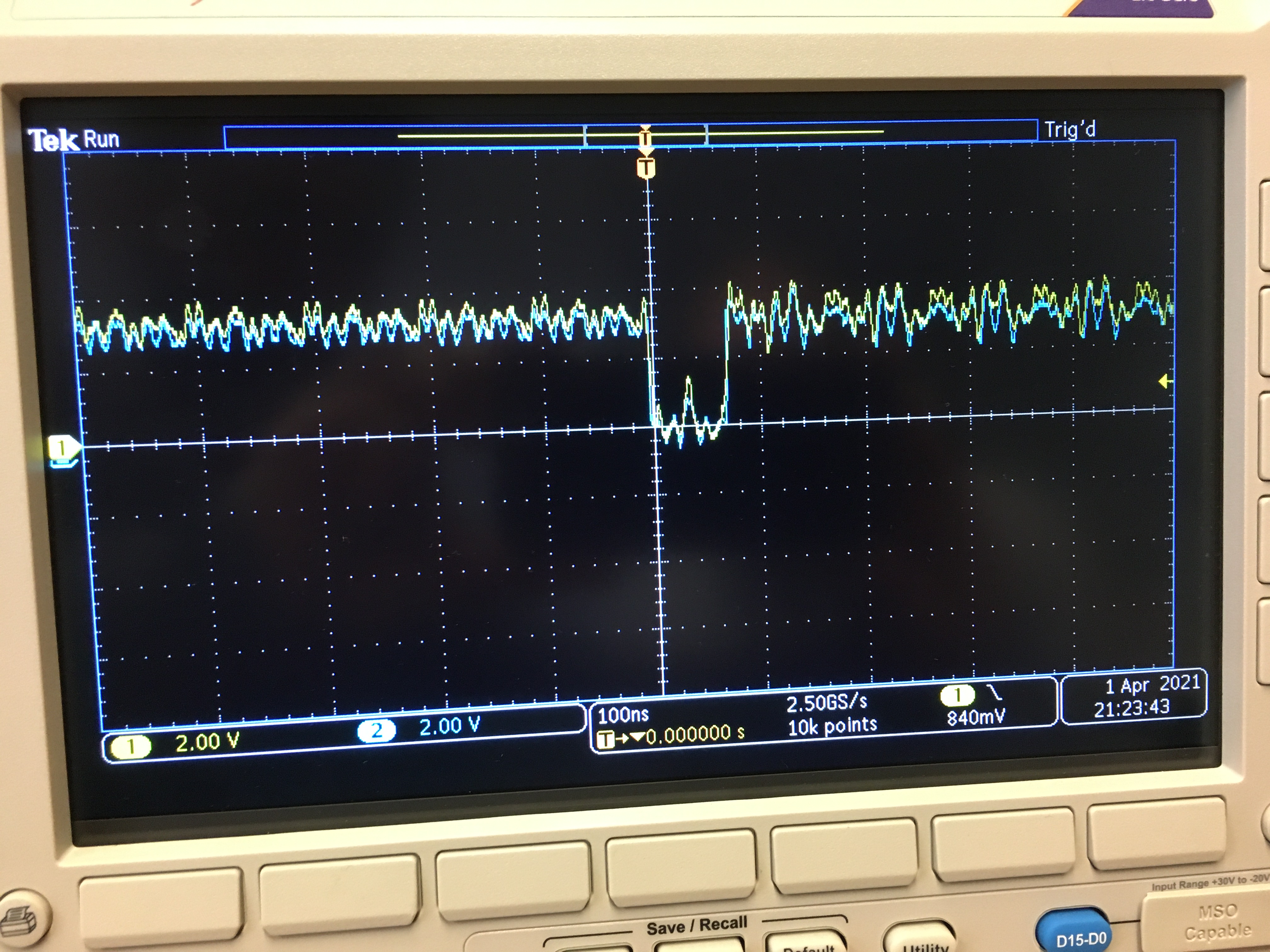
| 1 | P | Yellow trace shows DVALID at FPGA, blue shows DVALID at J2 of DDC232 board. | |
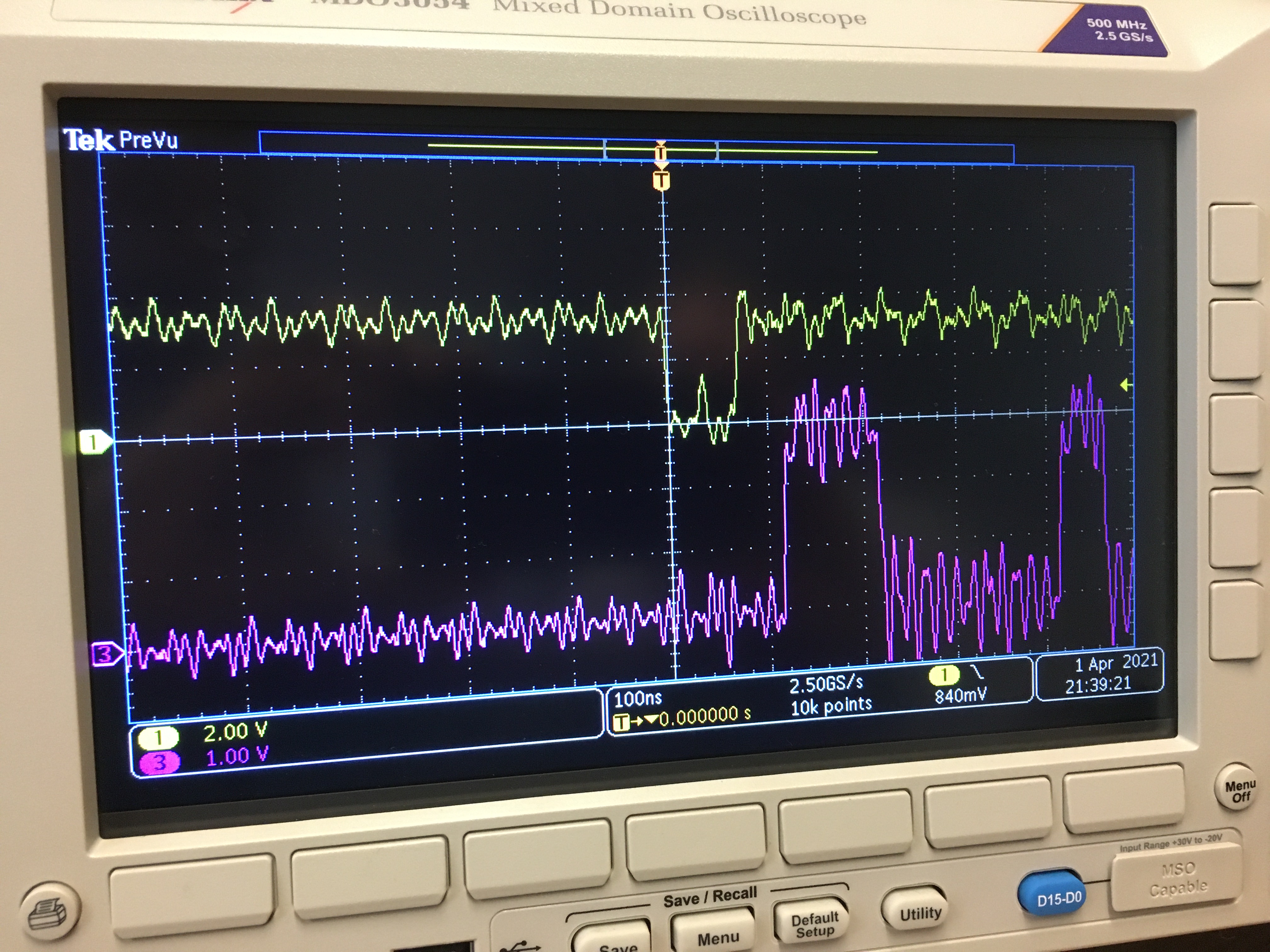
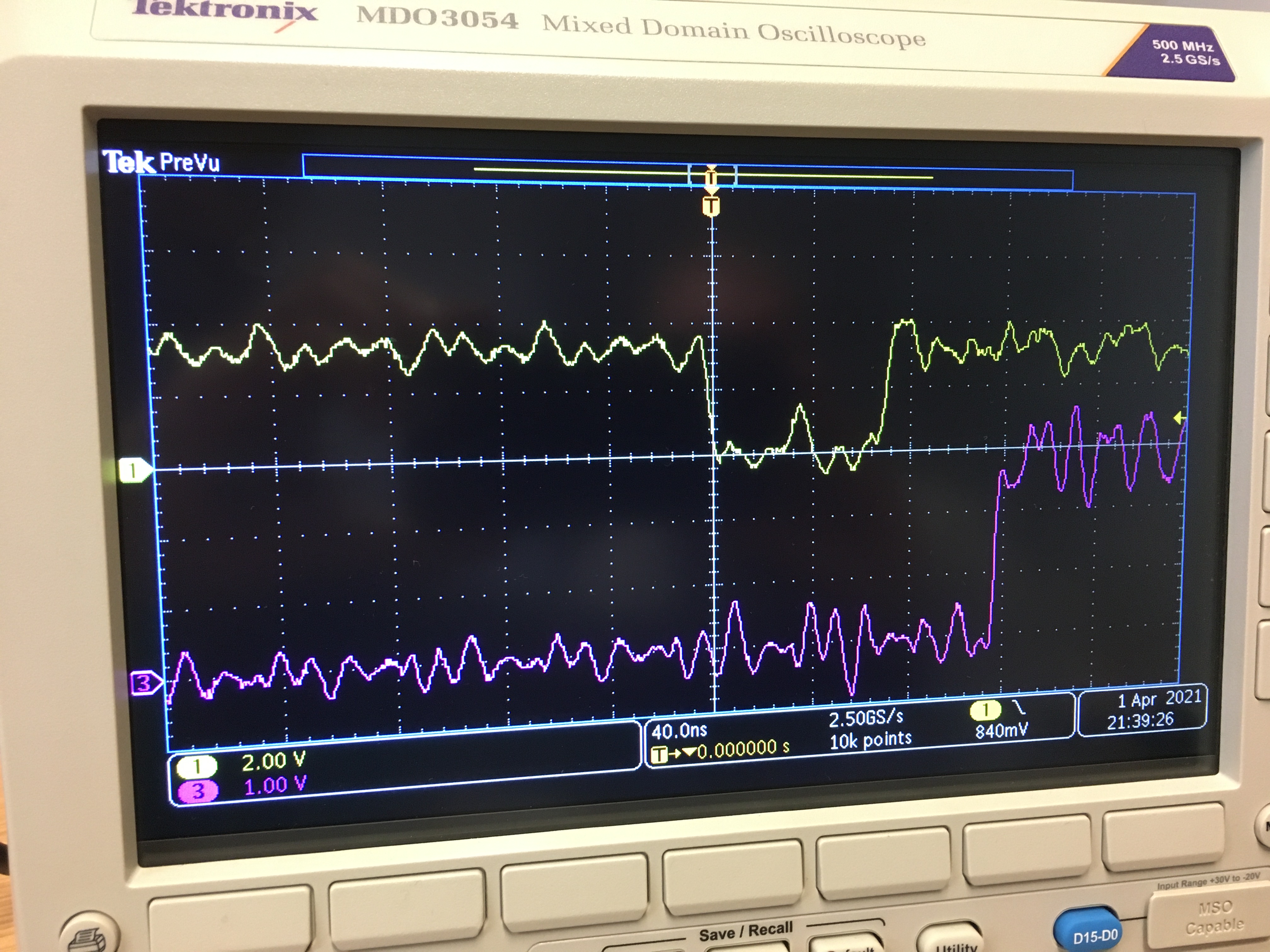
| 2 | P | Yellow trace shows DVALID at FPGA, green shows CLK at J2 of DDC232 board, purple shows 12V at J2 of DDC232 board. | |
| 3 | P | Yellow trace shows DVALID at FPGA, purple trace shows DOUT at J2 of DDC232 board. | |
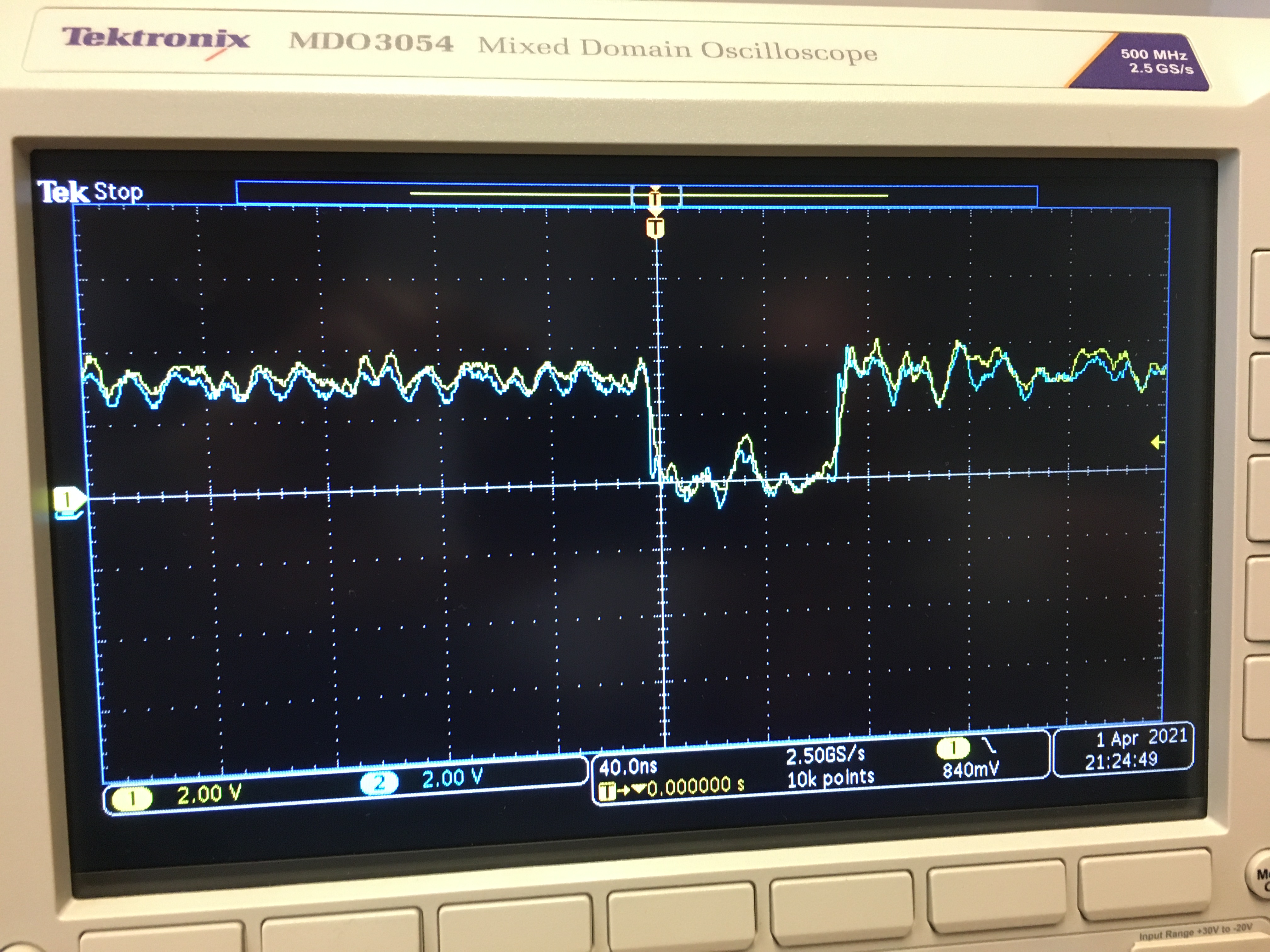
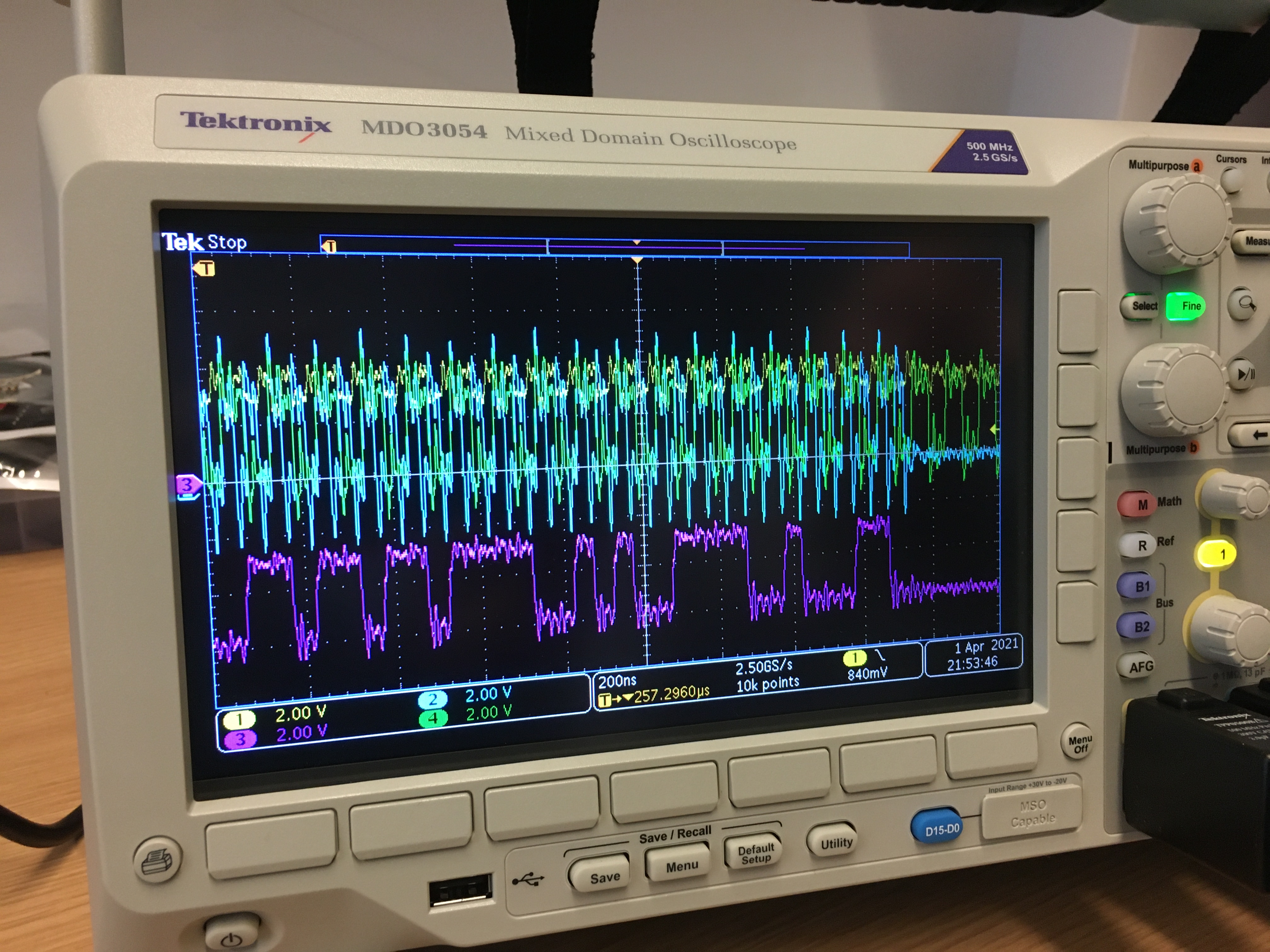
| 4 | P | Green trace shows CLK at J2 of DDC232 board, blue trace shows DCLK at J2 of DDC232 board. | |
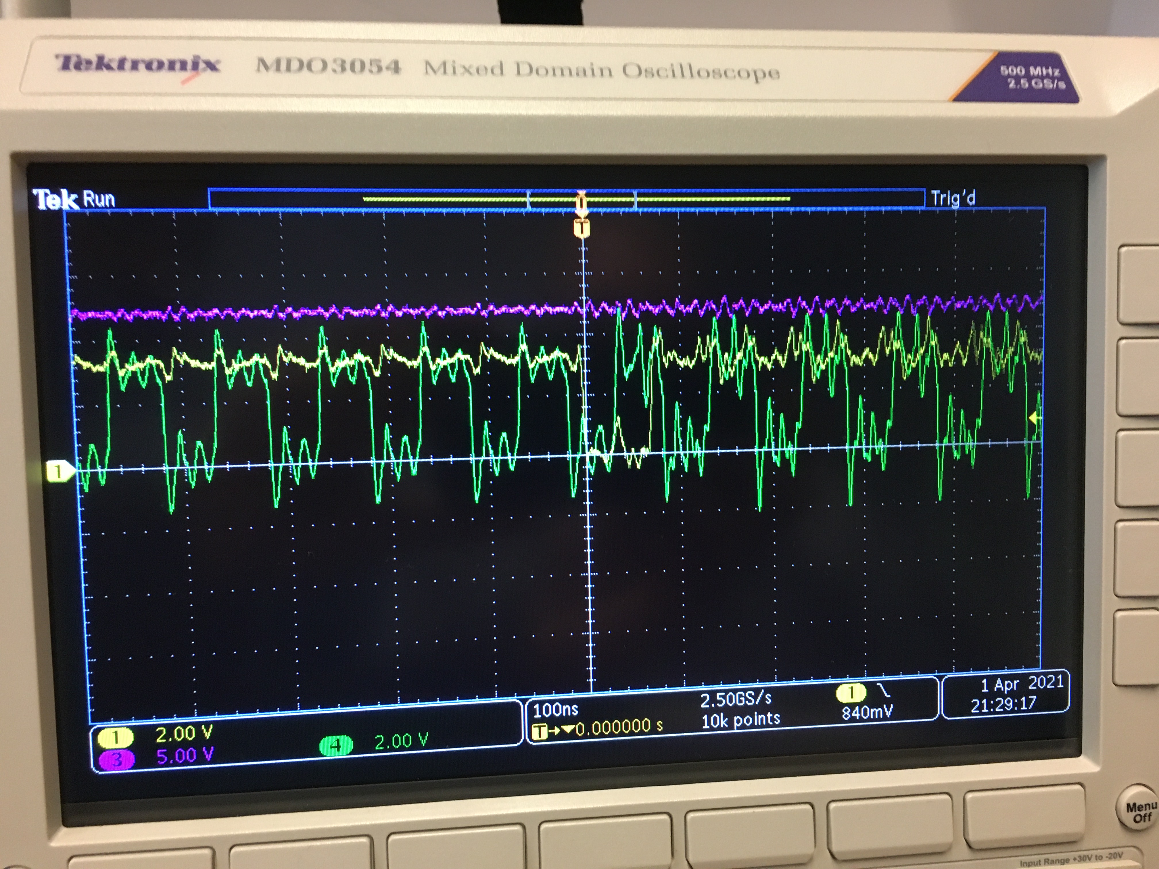
| 5 | P, P | Yellow trace shows DVALID at FPGA, green shows CLK of 1st board at J2, blue shows DCLK of 1st board at J2, purple shows 12V of 1st board at J2. | |
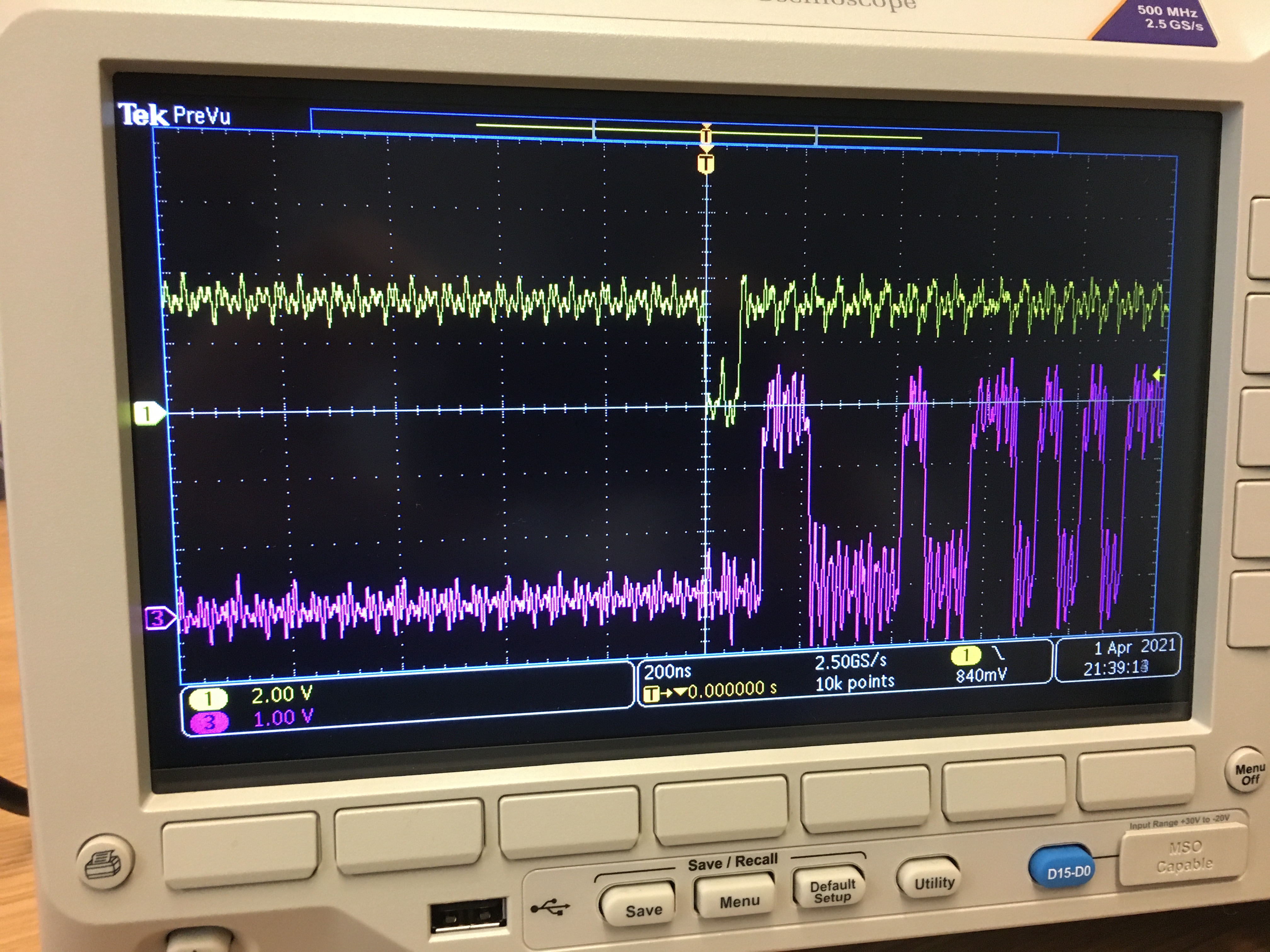
| 6 | P, P | Yellow trace shows DVALID at FPGA, green shows CLK of 1st board at J2, blue shows DCLK of 1st board at J2, purple shows DOUT of 1st board at J2. | |
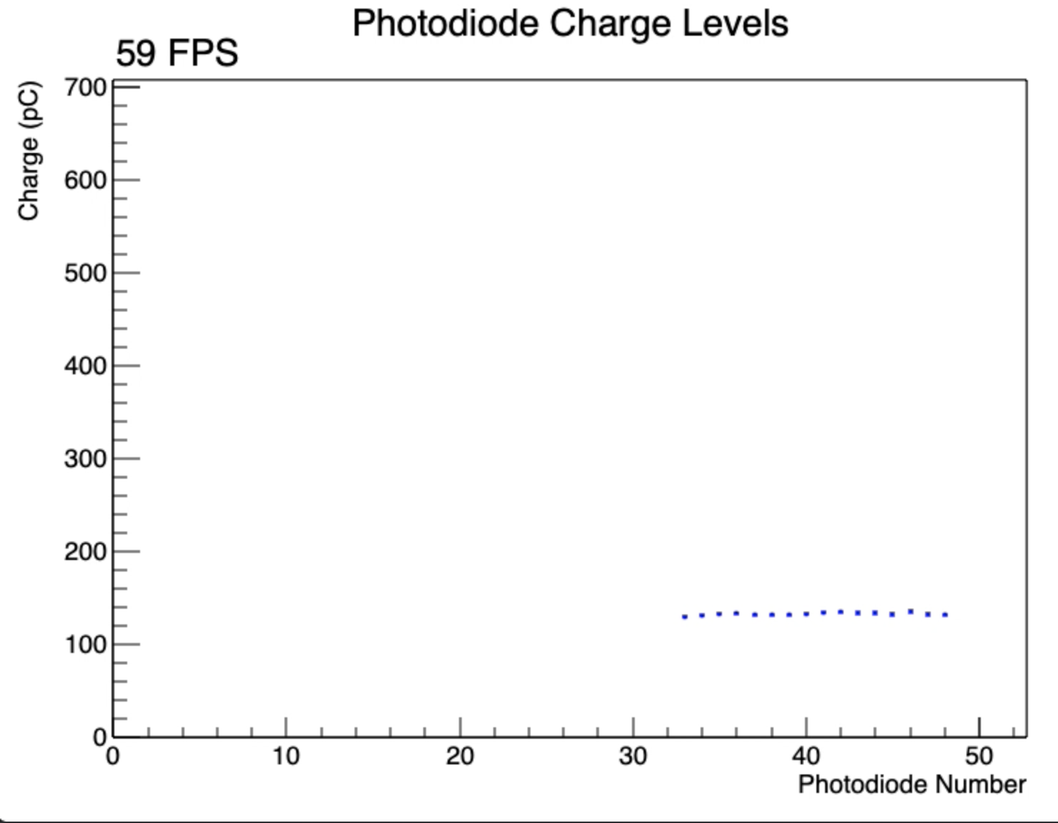
| 7 | 3, 4, 1 | Swept uncovering of each photodiode in turn - in opposite direction to run 6 - followed by board rotation and swept covering with finger. Note that board 4 shows zero output during uncovering due to signal dropouts associated with rotation. Low signals around 1m25s mark are a results of covering photodiodes partially with a finger. | |
| 8 | 4, 3, 1 | Swept uncovering of each photodiode in turn followed by board rotation and swept covering with finger. Repeat of run 7 above but with board reordering. Note that board 4 no longer shows noise when rotated now that its the last board in the chain. | |
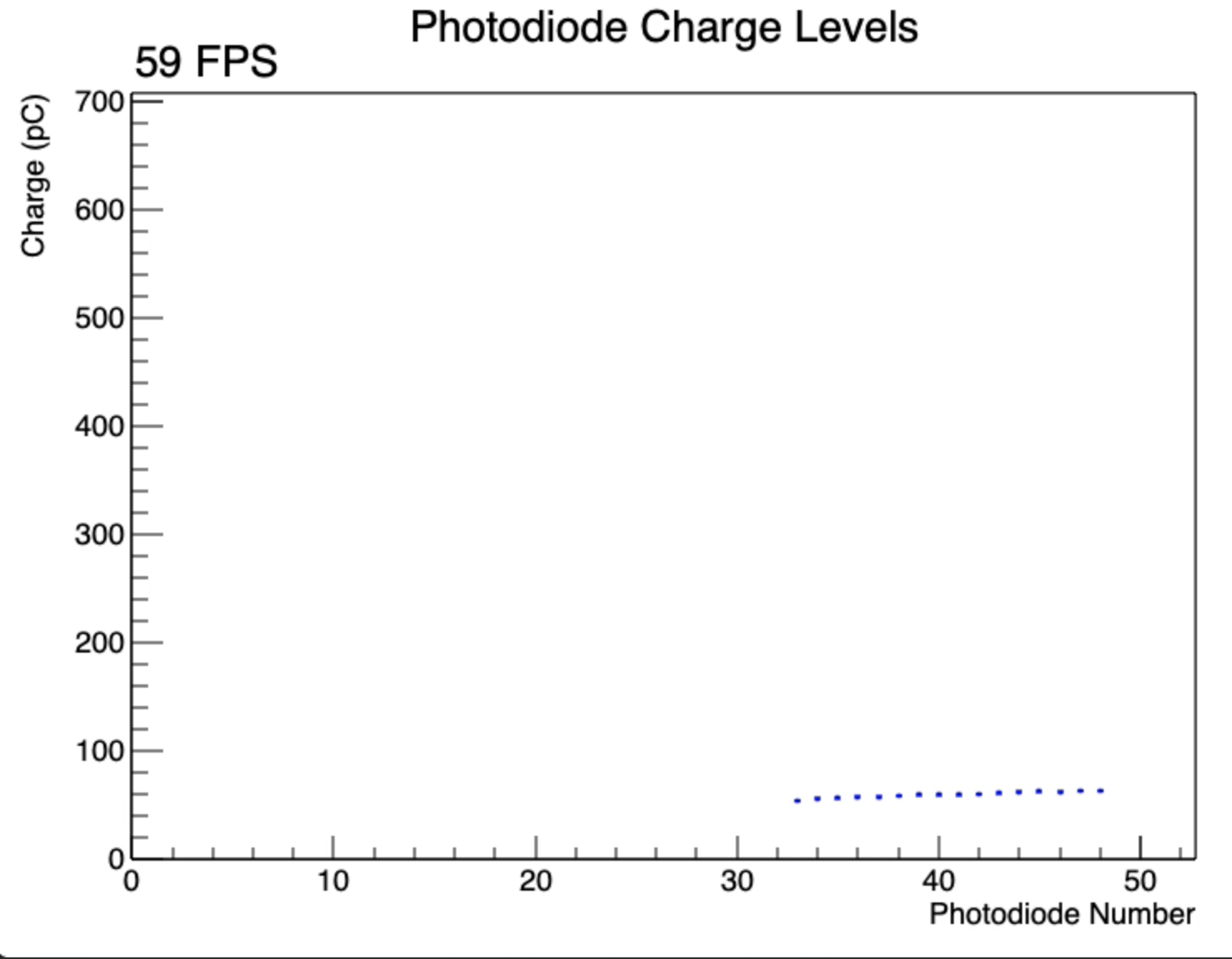
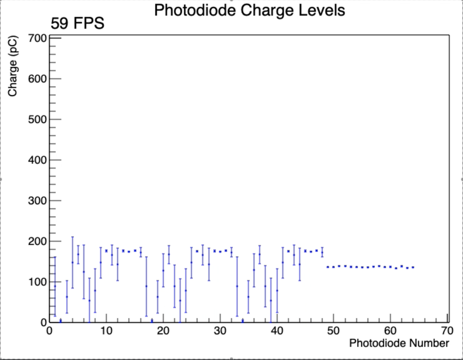
| 9 | 3, 4, 2 | Rotation of boards followed by swept covering of a few photodiodes in turn with black cloth. Now includes board 2 with resistor-shorted photodiode connections. Note that neither boards 4 or 2 show any output, corroborating that low values are mirrored despite board 4 being exposed to light. | |
| 10 | 3, 2, 4 | Rotation of boards followed by swept covering of a few photodiodes in turn with black cloth. Reording of boards from run 9 above: note that the behaviour is similar with no output from boards 2 and 4. | |
| 11 | 3, 1, 4, 2 | board rotation and sweep covering of photodiodes | |
| 12 | 3, 4, 2, 1 | board rotation and sweep covering of photodiodes | |
| 13 | 3, 2, 1, 4 | board rotation and sweep covering of photodiodes |
